| CPC H01L 24/05 (2013.01) [H01L 24/13 (2013.01); H01L 24/81 (2013.01); H01L 2224/02245 (2013.01); H01L 2224/02255 (2013.01); H01L 2224/0401 (2013.01); H01L 2224/13026 (2013.01); H01L 2224/81024 (2013.01); H01L 2224/81815 (2013.01); H01L 2924/13091 (2013.01)] | 18 Claims |

|
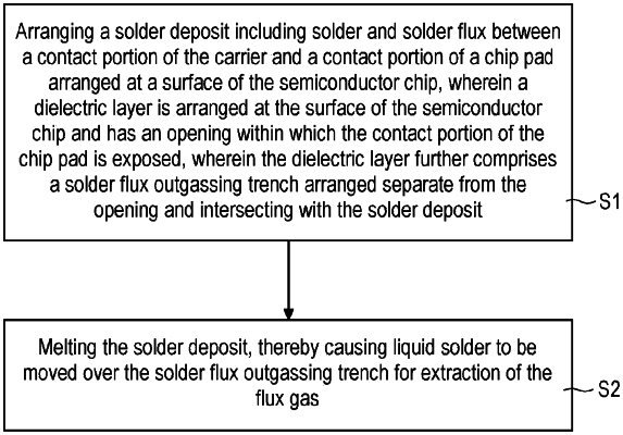
1. A method of soldering a semiconductor chip to a chip carrier, the method comprising:
arranging a solder deposit including solder and solder flux between a contact portion of the chip carrier and a contact portion of a chip pad arranged at a surface of the semiconductor chip, wherein a dielectric layer is arranged at the surface of the semiconductor chip and has an opening within which the contact portion of the chip pad is exposed, wherein the dielectric layer further comprises a solder flux outgassing trench arranged separate from the opening and intersecting with the solder deposit; and
melting the solder deposit which causes liquid solder to be moved over the solder flux outgassing trench for extraction of flux gas.
|