| CPC H01L 23/552 (2013.01) [H01L 21/568 (2013.01); H01L 23/49816 (2013.01); H01L 23/49838 (2013.01); H01L 24/16 (2013.01); H01L 2224/16227 (2013.01)] | 18 Claims |

|
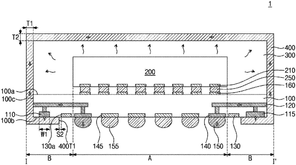
1. A semiconductor package, comprising:
a substrate including at least one ground pad and a ground terminal pad;
a semiconductor chip on the substrate;
a shield layer on the substrate and covering the semiconductor chip;
a ground terminal on a bottom surface of the ground terminal pad,
wherein:
the shield layer extends onto a bottom surface of the substrate and includes an opening region on the bottom surface of the substrate,
a bottom surface of the at least one ground pad is at the bottom surface of the substrate,
the shield layer on the bottom surface of the substrate is in contact with the bottom surface of the at least one ground pad, and
a distance between a sidewall of the at least one ground pad and the shield layer is shorter than a distance between a sidewall of the ground terminal pad and the shield layer; and
a test pad on the bottom surface of the substrate, wherein the test pad is aligned with the opening region of the shield layer such that the opening region of the shield layer exposes the test pad.
|