| CPC H01L 23/535 (2013.01) [H01L 21/76807 (2013.01); H01L 21/76829 (2013.01); H01L 21/76843 (2013.01); H01L 21/76895 (2013.01); H01L 23/485 (2013.01); H01L 29/0649 (2013.01); H01L 29/41791 (2013.01); H01L 29/66795 (2013.01); H01L 29/785 (2013.01); H01L 21/28518 (2013.01); H01L 21/76805 (2013.01); H01L 21/76831 (2013.01); H01L 29/165 (2013.01); H01L 29/66545 (2013.01); H01L 29/7848 (2013.01)] | 19 Claims |

|
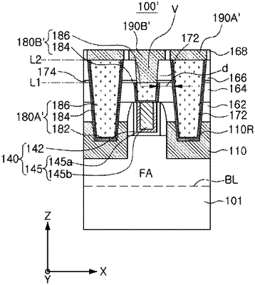
1. A semiconductor device comprising:
a substrate having an active region;
a plurality of active fins protruding from the active region and extending in a first direction;
a gate structure traversing the plurality of active fins and extending in a second direction intersecting the first direction;
a source/drain region disposed in the plurality of active fins at a side of the gate structure;
an inter-gate insulating layer covering the source/drain region disposed between the gate structure and another gate structure next to the gate structure;
a first etch stop layer conformally disposed on the gate structure;
a first interlayer insulating layer disposed on the first etch stop layer;
a second etch stop layer disposed on the first interlayer insulating layer;
a second interlayer insulating layer disposed on the gate structure and the source/drain region;
a first contact plug connected to the source/drain region through the first interlayer insulating layer, the first etch stop layer and the inter-gate insulating layer, and extending in the second direction;
a second contact plug connected to the gate structure through the first etch stop layer, the first interlayer insulating layer, the second etch stop layer and the second interlayer insulating layer;
a first metal line disposed on the second interlayer insulating layer, and having a metal via connected to a portion of the first contact plug through the second interlayer insulating layer and the second etch stop layer; and
a second metal line disposed on the second interlayer insulating layer, and directly connected to the second contact plug,
wherein a level of an upper surface of the second etch stop layer is higher than a level of an upper surface of the first contact plug, and is lower than a level of an upper surface of the second contact plug, and
a width of the first contact plug in the second direction is greater than a width of the metal via in the second direction.
|