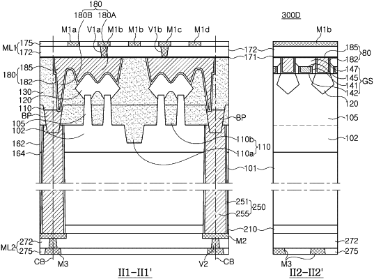
| CPC H01L 23/5286 (2013.01) [H01L 27/0207 (2013.01); H01L 27/092 (2013.01); H01L 29/42392 (2013.01); H01L 29/78696 (2013.01)] | 20 Claims |

|
1. A semiconductor device comprising:
a substrate having an active region;
a plurality of standard cells on the active region of the substrate, the plurality of standard cell arranged in a plurality of rows, the plurality of rows extending in a first direction, the plurality of standard cells each including
an active pattern extending in the first direction,
a gate structure intersecting the active pattern and extending in a second direction that intersects the first direction,
a plurality of source/drain regions in the active pattern with one of the plurality of source/drain regions on one side of the gate structure and another of the plurality of source/drain regions on another side of the gate structure, and
contact structures respectively connected to the source/drain regions;
a plurality of power supply lines disposed on a lower surface of the substrate;
a plurality of conductive through structure extending from the lower surface of the substrate toward an upper surface of the substrate, and respectively connected to the plurality of power supply lines; and
a plurality of buried power lines buried in the active region and respectively extending in the first direction along boundaries of the plurality of standard cells, the plurality of buried power lines respectively connected to the plurality of conductive through structure and supplying power to the plurality of standard cells through the conductive structures,
wherein each of the plurality of standard cells further includes a plurality of wiring lines extending in the first direction and arranged in the second direction, and
at least some wiring lines of the plurality of wiring lines in at least one standard cell among the plurality of standard cells are arranged such that at least one of a pitch, a spacing, or a line width is different from a respective one of a pitch, a spacing, or a line width of a neighboring standard cell.
|