| CPC H01L 23/5286 (2013.01) [H01L 23/528 (2013.01); H01L 23/552 (2013.01); H01L 24/05 (2013.01); H01L 24/46 (2013.01); H01L 25/0657 (2013.01); H01L 23/49816 (2013.01); H01L 24/48 (2013.01); H01L 2224/48 (2013.01); H01L 2224/48091 (2013.01); H01L 2224/48106 (2013.01); H01L 2224/48228 (2013.01); H01L 2225/0651 (2013.01); H01L 2225/06527 (2013.01); H01L 2225/06537 (2013.01); H01L 2225/06562 (2013.01); H01L 2225/06568 (2013.01); H01L 2924/15184 (2013.01); H01L 2924/15192 (2013.01); H01L 2924/15311 (2013.01)] | 10 Claims |

|
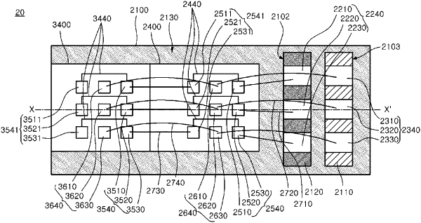
1. A semiconductor package comprising:
a package substrate including a first column of bond fingers arrayed in a first layer and a second column of bond fingers arrayed in a second layer;
a first semiconductor chip disposed on the package substrate to include a first column of chip pads arrayed in a first column, a second column of chip pads arrayed in a second column, a third column of chip pads arrayed in a third column located at one side of the second column opposite to the first column, and common interconnection lines for connecting the third column of chip pads to the first column of chip pads;
a second semiconductor chip disposed on the first semiconductor chip to include a first column of chip pads and a second column of chip pads;
first bonding wires connecting the first column of bond fingers to the first column of chip pads of the first semiconductor chip;
second bonding wires connecting the second column of bond fingers to the second column of chip pads of the first semiconductor chip;
third bonding wires connecting the first column of chip pads of the second semiconductor chip to the third column of chip pads of the first semiconductor chip; and
fourth bonding wires connecting the second column of chip pads of the second semiconductor chip to the second column of chip pads of the first semiconductor chip.
|