| CPC H01L 23/5286 (2013.01) [H01L 21/7806 (2013.01); H01L 21/8221 (2013.01); H01L 21/823871 (2013.01); H01L 27/0922 (2013.01)] | 7 Claims |

|
1. A CMOS structure comprising:
a wafer;
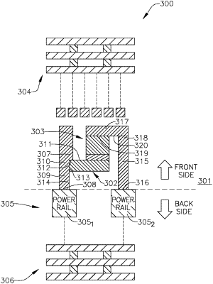
a first semiconductor device and a second semiconductor device on a front side of the wafer, the second semiconductor device being stacked on the first semiconductor device;
power rails on a back side of the wafer, the power rails being coupled to the first and second semiconductor devices;
a backside power distribution network (PDN) grid on the back side of the wafer, the backside PDN grid being coupled to the power rails; and
front-side signal routing lines on the front side of the wafer, the front-side signal routing lines being coupled to the first and second semiconductor devices and above the first and second semiconductor devices;
a first power via coupled to the power rails and directly coupled to an upper surface of the first semiconductor device;
a second power via coupled to the power rails; and
a power contact coupled to the second power via and to an upper surface of the second semiconductor device,
wherein the first power via comprises a narrower portion below the first semiconductor device and a wider portion above the first semiconductor device,
wherein the first semiconductor device and the second semiconductor device are configured to receive power only from the backside PDN grid.
|