| CPC H01L 23/5226 (2013.01) [H01L 21/76802 (2013.01); H01L 21/76877 (2013.01); H01L 21/76885 (2013.01); H01L 23/5283 (2013.01); H01L 29/41725 (2013.01); H01L 29/4232 (2013.01)] | 20 Claims |

|
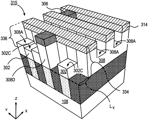
1. A method of fabricating an integrated circuit interconnect structure, the method comprising:
forming first and second parallel lines of conductive material, each line extending in a first direction with a first dielectric therebetween;
forming a stack structure over the first dielectric, the stack structure comprising a second dielectric and a third dielectric;
forming a fourth dielectric over the first and second lines;
patterning an opening in the third dielectric and extending in a second direction, orthogonal to the first direction, wherein the opening exposes a portion of the fourth dielectric;
forming a fifth dielectric in the opening and on the exposed portion of the fourth dielectric;
exposing a portion of each of the first and second lines by etching the fourth dielectric where not masked by the fifth dielectric; and
forming a conductive feature on the exposed portion of the first and second lines.
|