| CPC H01L 23/49503 (2013.01) [H01L 23/49541 (2013.01); H01L 23/49548 (2013.01); H01L 23/49565 (2013.01); H01L 24/48 (2013.01); H01L 24/49 (2013.01); H01L 2224/4801 (2013.01); H01L 2224/48245 (2013.01); H01L 2224/4845 (2013.01); H01L 2224/48455 (2013.01); H01L 2224/4903 (2013.01); H01L 2924/182 (2013.01); H01L 2924/183 (2013.01); H01L 2924/186 (2013.01)] | 17 Claims |

|
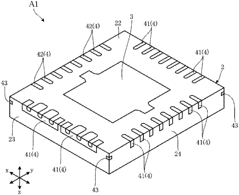
1. A semiconductor device, comprising:
a semiconductor element having an element main surface and an element back surface spaced apart from each other in a thickness direction and including a plurality of main surface electrodes arranged on the element main surface;
a die pad having a die pad main surface on which the semiconductor element is mounted;
a plurality of leads including at least one first lead arranged on one side in a first direction orthogonal to the thickness direction with respect to the die pad, and arranged around the die pad when viewed in the thickness direction;
a plurality of connecting members including a first connecting member bonded to the at least one first lead, and configured to electrically connect the plurality of main surface electrodes and the plurality of leads; and
a resin member configured to seal the semiconductor element, a part of the die pad, parts of the plurality of leads, and the plurality of connecting members,
wherein each of the plurality of leads is configured to entirely overlap with the resin member when viewed in the thickness direction and arranged along an outer edge of the resin member when viewed in the thickness direction,
wherein the die pad includes a first portion, a second portion, a third portion, and a fourth portion,
wherein the die pad main surface spans the first portion, the second portion, the third portion, and the fourth portion,
wherein the first portion has a first back surface facing a side opposite to the die pad main surface and overlaps with the semiconductor element when viewed in the thickness direction,
wherein the second portion has a second back surface facing a side opposite to the die pad main surface and located closer to the die pad main surface than the first back surface in the thickness direction, and is connected to an outer edge of the first portion when viewed in the thickness direction,
wherein the third portion has a third back surface facing a side opposite to the die pad main surface and being flush with the first back surface, and extends from one end edge of the first portion to one end edge of the die pad main surface in a second direction orthogonal to the thickness direction and the first direction, and
wherein the fourth portion has a fourth back surface facing a side opposite to the die pad main surface and being flush with the first back surface, and extends from the other end edge of the first portion to the other end edge of the die pad main surface in the second direction.
|