| CPC H01L 23/10 (2013.01) [H01L 23/047 (2013.01)] | 18 Claims |
|
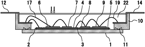
1. A semiconductor module comprising:
a base plate;
an insulating substrate provided on the base plate;
a semiconductor device provided on the insulating substrate;
a case arranged to surround the insulating substrate and the semiconductor device and bonded to the base plate with an adhesive; and
a sealant sealing the insulating substrate and the semiconductor device in the case,
wherein a groove is provided on a lower surface of the case opposing an upper surface peripheral portion of the base plate,
a bottom surface of the groove has a protruding part protruding toward the base plate,
the protruding part includes a vertex and gradients respectively provided closer to an inner side of the case and closer to an outer side of the case with the vertex sandwiched therebetween,
the adhesive contacts the vertex and is housed in the groove, and
an inner surface of the groove in the case and a region, to which the adhesive is applied, of the base plate are subjected to surface roughening processing.
|