| CPC H01L 22/30 (2013.01) [C30B 25/186 (2013.01); H01L 21/02002 (2013.01); H01L 21/02005 (2013.01); H01L 22/34 (2013.01); H10B 43/27 (2023.02)] | 11 Claims |
|
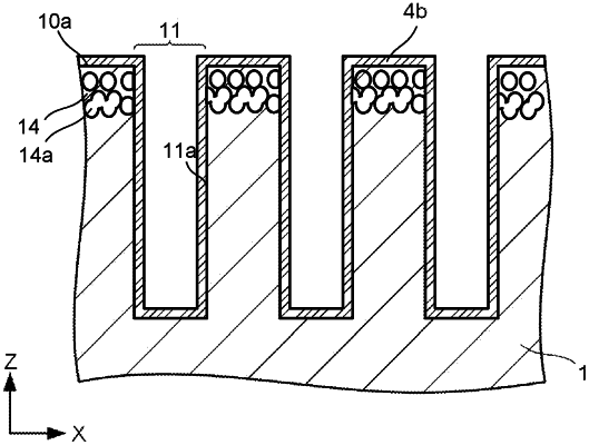
1. A semiconductor wafer, comprising:
a surface having at least one recess including an inner wall surface and a bottom surface, the inner wall surface and the bottom surface being exposed, wherein:
the at least one recess includes a first recess and a second recess;
the first recess extends along a first direction of the surface;
the second recess extends along a second direction intersecting with the first direction on the surface;
each of the first and second recesses is surrounded by the corresponding inner wall surface; and
the surface further has a porous region.
|