| CPC H01L 21/823814 (2013.01) [H01L 27/092 (2013.01); H01L 29/0673 (2013.01); H01L 29/401 (2013.01); H01L 29/42392 (2013.01); H01L 29/456 (2013.01); H01L 29/775 (2013.01); H01L 29/78696 (2013.01)] | 20 Claims |

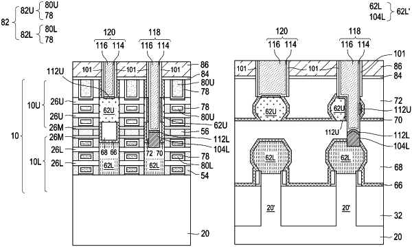
|
1. A method comprising:
forming Complementary Field-Effect Transistors comprising:
a lower transistor comprising a lower source/drain region; and
an upper transistor comprising an upper source/drain region;
etching an upper dielectric layer over the upper source/drain region and a lower dielectric layer between the upper source/drain region and the lower source/drain region to form an opening, wherein a sidewall of the upper source/drain region and a top surface of the lower source/drain region are exposed to the opening;
performing an epitaxy process to form:
a first semiconductor layer on the sidewall of the upper source/drain region; and
a second semiconductor layer on the top surface of the lower source/drain region;
removing the first semiconductor layer, with the second semiconductor layer being remaining, wherein the second semiconductor layer and the lower source/drain region collectively form a combined source/drain region; and
forming a contact plug in the opening, wherein the contact plug electrically connects the upper source/drain region to the combined source/drain region.
|