US 12,131,952 B2
Wafer dicing using femtosecond-based laser and plasma etch
Wei-Sheng Lei, San Jose, CA (US); Brad Eaton, Menlo Park, CA (US); Madhava Rao Yalamanchili, Morgan Hill, CA (US); Saravjeet Singh, Santa Clara, CA (US); Ajay Kumar, Cupertino, CA (US); and James M. Holden, San Jose, CA (US)
Assigned to Applied Materials, Inc., Santa Clara, CA (US)
Filed by Applied Materials, Inc., Santa Clara, CA (US)
Filed on Mar. 2, 2023, as Appl. No. 18/116,736.
Application 14/476,060 is a division of application No. 14/146,887, filed on Jan. 3, 2014, granted, now 8,853,056, issued on Oct. 7, 2014.
Application 18/116,736 is a continuation of application No. 17/137,099, filed on Dec. 29, 2020, granted, now 11,621,194.
Application 17/137,099 is a continuation of application No. 16/885,142, filed on May 27, 2020, granted, now 10,910,271, issued on Feb. 2, 2021.
Application 16/885,142 is a continuation of application No. 16/706,541, filed on Dec. 6, 2019, granted, now 10,714,390, issued on Jul. 14, 2020.
Application 16/706,541 is a continuation of application No. 16/193,886, filed on Nov. 16, 2018, granted, now 10,566,238, issued on Feb. 18, 2020.
Application 16/193,886 is a continuation of application No. 15/005,700, filed on Jan. 25, 2016, granted, now 10,163,713, issued on Dec. 25, 2018.
Application 15/005,700 is a continuation of application No. 14/476,060, filed on Sep. 3, 2014, granted, now 9,245,802, issued on Jan. 26, 2016.
Application 14/146,887 is a continuation of application No. 13/160,713, filed on Jun. 15, 2011, granted, now 8,642,448, issued on Feb. 4, 2014.
Claims priority of provisional application 61/357,468, filed on Jun. 22, 2010.
Prior Publication US 2023/0207393 A1, Jun. 29, 2023
This patent is subject to a terminal disclaimer.
Int. Cl. H01L 21/00 (2006.01); B23K 26/36 (2014.01); H01J 37/32 (2006.01); H01L 21/3065 (2006.01); H01L 21/308 (2006.01); H01L 21/67 (2006.01); H01L 21/78 (2006.01); H01L 21/822 (2006.01); H01L 23/544 (2006.01); H01L 21/683 (2006.01)
CPC H01L 21/822 (2013.01) [B23K 26/36 (2013.01); H01J 37/32889 (2013.01); H01J 37/32899 (2013.01); H01L 21/3065 (2013.01); H01L 21/3083 (2013.01); H01L 21/67069 (2013.01); H01L 21/67207 (2013.01); H01L 21/78 (2013.01); H01L 23/544 (2013.01); H01L 21/67092 (2013.01); H01L 21/6836 (2013.01); H01L 2221/68327 (2013.01); H01L 2924/0002 (2013.01)] 9 Claims
OG exemplary drawing
 
1. A system for dicing a semiconductor wafer comprising a plurality of integrated circuits, the system comprising:
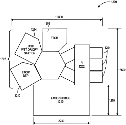
a cluster tool comprising a plasma etch chamber, and a robotic transfer chamber coupled to the plasma etch chamber, the cluster tool having a footprint;
a load lock;
a laser scribe apparatus, wherein the laser scribe apparatus is not included in the cluster tool, the laser scribe apparatus having a footprint; and
a factory interface coupled to the robotic transfer chamber of the cluster tool by the load lock, and the factory interface coupled to the laser scribe apparatus, wherein the factory interface comprises a robot with an arm or a blade, wherein a semiconductor wafer is transferred from the laser scribe apparatus to the robot of the factory interface, from the robot of the factory interface to the load lock, from the load lock to the robotic transfer chamber, and from the robotic transfer chamber to the plasma etch chamber, the factory interface having a footprint, wherein the footprint of the laser scribe apparatus is laterally overlapping with both the footprint of the cluster tool and the footprint of the factory interface.