| CPC H01L 21/67288 (2013.01) [G06T 7/0004 (2013.01); G06T 7/11 (2017.01); G06T 7/70 (2017.01); G06T 7/90 (2017.01); G06T 2207/10024 (2013.01); G06T 2207/30148 (2013.01)] | 16 Claims |

|
1. A wafer inspection method comprising:
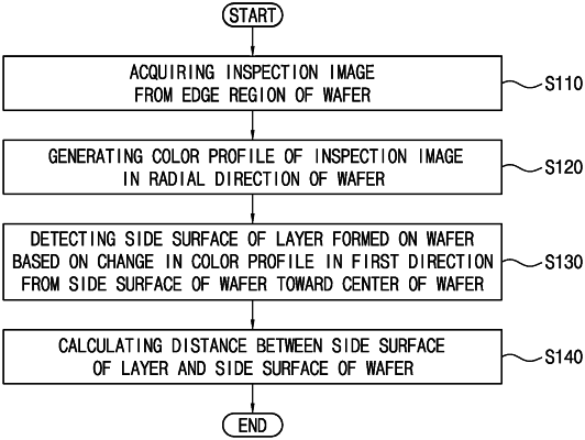
acquiring an inspection image from an edge region of a wafer;
generating a color profile of the inspection image in a radial direction of the wafer; and
detecting a side surface of a layer formed on the wafer based on a change in the color profile in a first direction from a side surface of the wafer toward a center of the wafer,
wherein the detecting the side surface of the layer comprises:
selecting one color from among red, green and blue according to a color of the layer;
searching a color ratio profile corresponding to the selected color from among the color ratio profiles in the first direction to detect a pixel having a predetermined color ratio of the selected color; and
searching the color ratio profile in the first direction from the detected pixel to detect a second pixel having the predetermined color ratio of the selected color when a color level value of the selected color of the detected pixel or a gray level value of the detected pixel is lower than a predetermined value.
|