| CPC H01L 21/02527 (2013.01) [C23C 16/26 (2013.01); C23C 16/50 (2013.01); H01L 21/02422 (2013.01); H01L 21/02425 (2013.01); H01L 21/0262 (2013.01); H01L 29/1606 (2013.01)] | 26 Claims |

|
1. A graphene structure comprising:
a substrate,
a material of the substrate including a semiconductor material, a metal material, or an inorganic insulating material; and
a directly grown graphene that is directly grown on a surface of the substrate and has a controlled surface energy, wherein
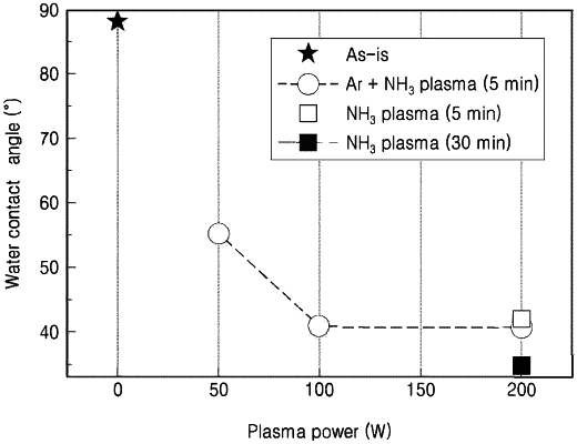
the directly grown graphene has a water contact angle of less than or equal to about 60 degrees with respect to the surface of the substrate, and
the directly grown graphene is directly on the material of the substrate such that the directly grown graphene is in contact with the semiconductor material, the metal material, or the inorganic insulating material of the substrate, and
the directly grown graphene has a domain size of greater than 0 nm and less than or equal to 100 nm.
|