| CPC H01G 4/30 (2013.01) [C04B 35/468 (2013.01); H01G 2/065 (2013.01); H01G 4/008 (2013.01); H01G 4/012 (2013.01); H01G 4/1227 (2013.01); C04B 2235/66 (2013.01)] | 13 Claims |

|
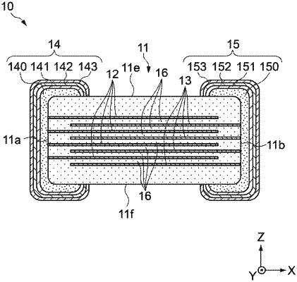
1. A multi-layer ceramic electronic component, comprising:
a ceramic body including internal electrodes laminated and drawn to a surface of the ceramic body; and
an external electrode including
a base film disposed on the surface of the ceramic body, connected to the internal electrodes, and formed from an electrically conductive material,
a first nickel film disposed on and in contact with the base film in a thickness direction of the base film, and
a second nickel film disposed on the first nickel film in a thickness direction of the first nickel film,
wherein a surface of the first nickel film is oxidized, forming an oxide film between the first nickel film and the second nickel film.
|