| CPC H01G 4/30 (2013.01) [H01G 4/008 (2013.01); H01G 4/232 (2013.01); H01G 4/248 (2013.01)] | 26 Claims |

|
1. A multilayer ceramic electronic component, comprising:
a ceramic body including a dielectric layer and first and second internal electrodes disposed to be alternately stacked with the dielectric layer interposed therebetween;
a first external electrode connected to the first internal electrode of the ceramic body; and
a second external electrode connected to the second internal electrode,
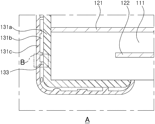
wherein the first external electrode comprises a first electrode layer disposed to be in contact with the ceramic body, a first conductive layer disposed on the first electrode layer, and a first metal layer disposed on the first conductive layer and in contact with the first electrode layer,
wherein the second external electrode comprises a second electrode layer disposed to be in contact with the ceramic body, a second conductive layer disposed on the second electrode layer, and a second metal layer disposed on the second conductive layer and in contact with the second electrode layer,
wherein the first conductive layer and the second conductive layer are plating layers, and
wherein at least one of the first conductive layer or the second conductive layer includes a non-corner/non-edge portion which is porous.
|