| CPC H01F 27/29 (2013.01) [H01F 27/2823 (2013.01); H01F 41/06 (2013.01)] | 5 Claims |

|
1. An electronic component comprising:
a leadout electrode portion provided on an outer surface of an element main body; and
a resin electrode layer formed at a part of the outer surface of the element main body and connected to the leadout electrode portion,
wherein the leadout electrode portion contains copper as a main component,
the resin electrode layer includes a conductor powder containing silver, and a resin,
the conductor powder contains first particles having an average particle size of 1 μm to 10 μm and second particles having an average particle size of 5 nm to 30 nm,
a diffusion layer containing copper oxide and silver is formed at an interface with the leadout electrode portion in the resin electrode layer,
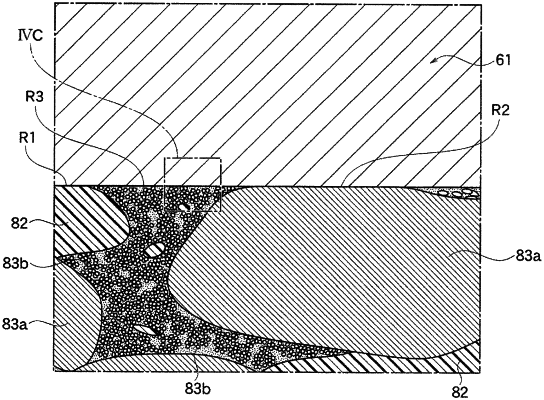
a first region (R1) where a resin component is in contact with an outermost surface of the leadout electrode portion, a second region (R2) where the first particles are in contact with the outermost surface, and a third region (R3) where the second particles are in contact with the outermost surface exist at the interface, and
the diffusion layer exists in the third region (R3) and is intermittently formed along the interface.
|