| CPC G11C 7/1057 (2013.01) [G06F 11/1076 (2013.01)] | 20 Claims |
|
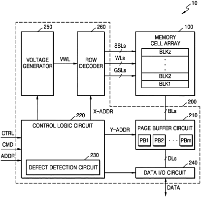
1. A non-volatile memory device comprising:
a memory cell array comprising a plurality of cell strings, each comprising a plurality of memory cells respectively connected to a plurality of word lines;
a page buffer circuit comprising a plurality of page buffers respectively connected to the plurality of memory cells through a plurality of bit lines, wherein a first page buffer from among the plurality of page buffers is connected to a first cell string from among the plurality of cell strings through a first bit line from among the plurality of bit lines;
a control logic circuit configured to control a pre-sensing operation to disconnect the first bit line and the first cell string from each other during a pre-sensing period for detecting a defect of the first bit line and control a post-sensing operation to connect the first bit line and the first cell string to each other in a post-sensing period for detecting defects of the plurality of word lines and the first bit line; and
a defect detection circuit configured to detect defects of the plurality of word lines based on a result of the pre-sensing operation and a result of the post-sensing operation.
|