| CPC G11C 5/025 (2013.01) [G11C 5/063 (2013.01); G11C 8/14 (2013.01); H10B 12/488 (2023.02)] | 25 Claims |

|
1. An apparatus comprising:
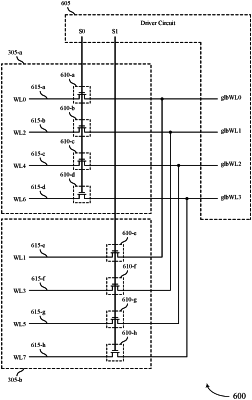
a plurality of word line conductors arranged in a stack along a first direction away from a substrate of a memory die, each word line conductor of the plurality of word line conductors extending along a second direction over the substrate and operable to access a respective set of one or more memory cells over the substrate;
a plurality of first portions of a semiconductor material over the substrate, each first portion of the plurality of first portions having a respective location along the first direction that is different than the respective location of one or more other first portions of the plurality of first portions, and each first portion of the plurality of first portions electrically coupled with a respective word line conductor of the plurality of word line conductors; and
a plurality of gate material portions over the substrate, each gate material portion of the plurality of gate material portions operable to modulate a conductivity between a respective first portion of the semiconductor material and a respective second portion of a plurality of second portions of the semiconductor material based at least in part on a voltage of the gate material portion.
|