| CPC G11C 16/16 (2013.01) [H01L 23/481 (2013.01); H01L 29/42328 (2013.01); H10B 41/10 (2023.02); H10B 41/27 (2023.02)] | 16 Claims |

|
1. A memory cell array, comprising:
a plurality of memory cells arranged in rows and columns, wherein respective ones of the memory cells includes spaced apart source and drain regions formed in a semiconductor substrate with a channel region extending there between, a floating gate disposed over and insulated from a first portion of the channel region, a select gate disposed over and insulated from a second portion of the channel region, and an erase gate disposed over and insulated from the source region;
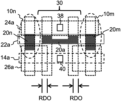
a strap region disposed between a first plurality of columns of the memory cells and a second plurality of columns of the memory cells; and
for one of the rows of the memory cells:
a dummy floating gate disposed in the strap region, over and insulated from the substrate, and between two of the memory cells in the one row of the memory cells, and
a first erase gate line electrically connecting together the erase gates of the memory cells in the one row of the memory cells and in the first plurality of columns of the memory cells, wherein the first erase gate line is aligned with the dummy floating gate with a first row direction gap between the first erase gate line and the dummy floating gate.
|