| CPC G11C 16/16 (2013.01) [G11C 7/04 (2013.01); G11C 16/08 (2013.01); G11C 16/24 (2013.01); G11C 16/26 (2013.01); G11C 16/349 (2013.01)] | 20 Claims |

|
1. A memory chip controller comprising:
one or more substrates, and
logic coupled to the one or more substrates, wherein the logic is implemented at least partly in one or more of configurable or fixed-functionality hardware, the logic to:
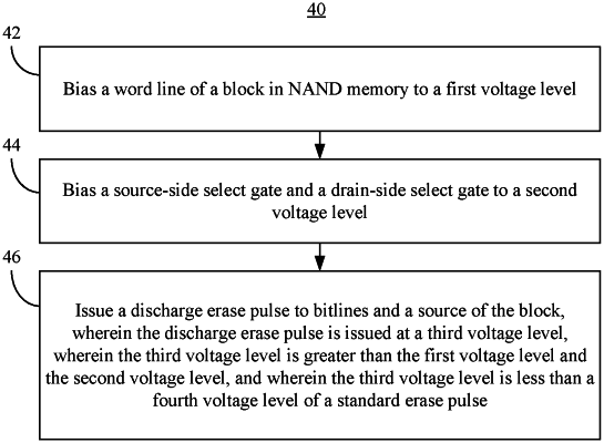
bias a word line of a block in NAND memory to a first voltage level,
bias a source-side select gate and a drain-side select gate of the block to a second voltage level, and
issue a discharge erase pulse to bitlines and a source of the block, wherein the discharge erase pulse is issued at a third voltage level, wherein the third voltage level is greater than the first voltage level and the second voltage level, and wherein the third voltage level is less than a fourth voltage level of a standard erase pulse.
|