| CPC G11C 16/16 (2013.01) [G11C 5/063 (2013.01); G11C 16/08 (2013.01); G11C 16/26 (2013.01); G11C 16/30 (2013.01)] | 20 Claims |
|
1. A non-volatile memory device comprising:
a plurality of word lines stacked above a substrate in a vertical direction, the plurality of word lines including a word line cut region;
a plurality of erase control lines spaced apart from each other in a first direction and extending in a second direction orthogonal to the first direction, wherein a first group of the plurality of erase control lines are relatively close to the word line cut region compared to a second group of the plurality of erase control lines that is relatively far from the word line cut region;
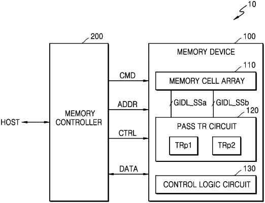
a pass transistor circuit comprising a first pass transistor and a second pass transistor, the first pass transistor being connected to the first group of the plurality of erase control lines, and the second pass transistor being connected to the second group of the plurality of erase control lines; and
a memory cell array including a plurality of blocks,
each block among the plurality of blocks including a plurality of channel structures connected to the plurality of word lines and the plurality of erase control lines, and
each of the plurality of channel structures extending in the vertical direction.
|