| CPC G11C 11/4096 (2013.01) [G11C 11/4094 (2013.01); G11C 16/24 (2013.01); H10B 12/20 (2023.02); G11C 2211/401 (2013.01)] | 15 Claims |

|
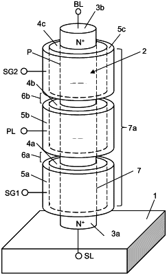
1. A memory device comprising a memory block constituted by a plurality of pages arranged in a column direction, each of the pages being constituted by a plurality of memory cells arranged in a row direction on a substrate,
each of the memory cells included in each of the pages comprising:
a semiconductor base material that stands on the substrate in a vertical direction or that extends along the substrate in a horizontal direction;
a first impurity layer and a second impurity layer that are disposed at respective ends of the semiconductor base material;
a first gate insulating layer that partially or entirely surrounds a side surface of the semiconductor base material between the first impurity layer and the second impurity layer and that is in contact with or in close vicinity to the first impurity layer;
a second gate insulating layer that surrounds the side surface of the semiconductor base material, that is connected to the first gate insulating layer, and that is in contact with or in close vicinity to the second impurity layer;
a first gate conductor layer that partially or entirely covers the first gate insulating layer;
a second gate conductor layer that covers the second gate insulating layer; and
a channel semiconductor layer that is the semiconductor base material and that is covered by the first gate insulating layer and the second gate insulating layer, wherein
the first impurity layer of each of the memory cells is connected to a source line, the second impurity layer thereof is connected to a corresponding one of bit lines, one of the first gate conductor layer or the second gate conductor layer thereof is connected to a corresponding one of word lines, the other of the first gate conductor layer or the second gate conductor layer thereof is connected to a corresponding one of driving control lines, and each of the bit lines is connected to a corresponding one of sense amplifier circuits,
an operation of retaining a group of positive holes, inside the channel semiconductor layer, generated by an impact ionization phenomenon, by controlling voltages applied to the first gate conductor layer, the second gate conductor layer, the first impurity layer, and the second impurity layer is performed,
a page write operation of making a voltage of the channel semiconductor layer be equal to a first data retention voltage that is higher than the voltage of either the first impurity layer or the second impurity layer or that is higher than the voltages of both the first impurity layer and the second impurity layer is performed,
a page erase operation of discharging the group of positive holes through either the first impurity layer or the second impurity layer or both the first impurity layer and the second impurity layer by controlling the voltages applied to the first impurity layer, the second impurity layer, the first gate conductor layer, and the second gate conductor layer, and subsequently, making the voltage of the channel semiconductor layer be equal to a second data retention voltage that is lower than the first data retention voltage by capacitive coupling between the first gate conductor layer and the channel semiconductor layer and capacitive coupling between the second gate conductor layer and the channel semiconductor layer is performed,
a page read operation of reading page data of a group of memory cells in a selected page among the pages to the bit lines is performed, and
in the page write operation and in the page read operation, a selected driving control line among the driving control lines is lowered to zero volt at a first reset time that is after an end of page writing and an end of page reading, the driving control line is isolated from a driving circuit at a second reset time that is after the first reset time to thereby put the driving control line in a zero-volt floating state, and a selected word line among the word lines is set at zero volt at a third reset time that is after the second reset time to thereby put the driving control line in a negative-voltage floating state by capacitive coupling between the word line and the driving control line.
|