| CPC G09G 3/3233 (2013.01) [G09G 2310/061 (2013.01); G09G 2310/08 (2013.01); G09G 2320/0214 (2013.01); G09G 2320/0233 (2013.01)] | 20 Claims |

|
1. A display panel, comprising: a pixel circuit and a light-emitting diode; wherein
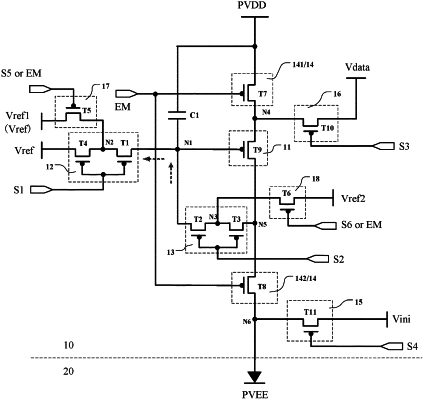
the pixel circuit comprises a drive circuit, a reset circuit and a compensation circuit, wherein
the drive circuit is configured to provide a drive current for the light-emitting diode, the drive circuit comprises a drive transistor, and a gate of the drive transistor is connected to a first node;
the reset circuit is configured to provide a reset signal for the gate of the drive transistor, and the reset circuit comprises a first transistor, wherein one end of the first transistor is connected to the first node, and another end of the first transistor is connected to a second node;
the compensation circuit is configured to compensate for a threshold voltage of the drive transistor, and the compensation circuit comprises a second transistor and a third transistor, wherein a connection node between the second transistor and the third transistor is a third node, and another end of the second transistor is connected to the first node; and
the display panel comprises a plurality of refresh frames,
wherein in at least one refresh frame of the plurality of refresh frames,
in a first stage comprised in a working process of the pixel circuit, the first transistor and the second transistor are turned off, and a voltage V1 of the first node, a voltage V2 of the second node and a voltage V3 of the third node satisfy that V1−V2=K(V3−V2), wherein K denotes a fixed value, and 0<K<1, such that a voltage difference between V1 and V2 is less than a voltage difference between V3 and V2, and a ratio of the voltage difference between V1 and V2 to the voltage difference between V3 and V2 is fixed;
wherein the third node is further connected to a second signal terminal, a second signal Vref2 provided by the second terminal satisfies that V1−V2=K (Vref2−V2).
|