| CPC G06V 40/1306 (2022.01) [G06F 3/04164 (2019.05); G06F 3/0445 (2019.05); G06F 3/0446 (2019.05); G06K 19/0718 (2013.01); G06V 40/1329 (2022.01); G06F 2203/04103 (2013.01)] | 20 Claims |

|
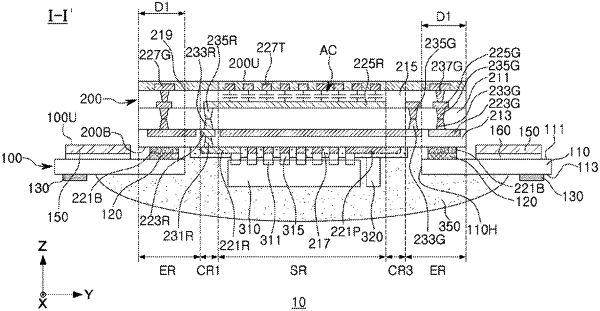
1. A fingerprint sensor package comprising:
a first substrate comprising:
a core insulating layer having a first surface and a second surface opposing each other, the first substrate having a through-hole penetrating through the first surface and the second surface,
a first bonding pad along a circumference of the through-hole on the first surface, and
an external connection pad on an edge of the second surface;
a second substrate comprising:
a third surface and a fourth surface opposing each other,
a plurality of first sensing patterns spaced apart from each other in a first direction and extending in a second direction intersecting the first direction,
a plurality of second sensing patterns spaced apart from each other in the second direction and extending in the first direction, on the third surface, and
a second bonding pad on an edge of the fourth surface and bonded to the first bonding pad, the second substrate having an overlapping region covering the through-hole and overlapping the edge of the second surface;
a controller chip on the fourth surface of the second substrate and accommodated in the through-hole of the first substrate; and
a molded layer filling the through-hole on the second surface of the core insulating layer, covering the controller chip, and spaced apart from the external connection pad.
|