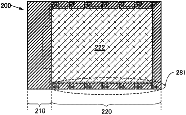
| CPC G06F 3/14 (2013.01) [G06F 1/1615 (2013.01); G06F 1/1652 (2013.01); G06F 3/147 (2013.01); G09G 5/14 (2013.01); G09G 2320/0686 (2013.01); G09G 2340/04 (2013.01); G09G 2340/0407 (2013.01); G09G 2380/02 (2013.01)] | 14 Claims |

|
1. A semiconductor device comprising:
a bendable touch panel, the bendable touch panel comprising:
a display portion;
a touch sensor overlapping with the display portion; and
a bending member comprising a plurality of hinge components,
wherein a barrier film is provided over a resin layer comprising polyimide,
wherein a first conductive film is provided over the barrier film,
wherein a first insulating film is provided over the first conductive film,
wherein a semiconductor layer is provided over the first insulating film,
wherein a second conductive film is provided over and electrically connected to the semiconductor layer,
wherein a second insulating film is provided over the second conductive film,
wherein a light-emitting element is provided over the second insulating film,
wherein a third insulating film is provided so as to cover a top surface and a side surface of a first electrode of the light-emitting element,
wherein a second electrode of the light-emitting element is provided over the third insulating film,
wherein the touch sensor is provided over the second electrode of the light-emitting element,
wherein a layer comprising a polarizing plate is provided over the touch sensor,
wherein the bendable touch panel is supported by the bending member,
wherein the display portion comprises a first region, a second region, and a third region,
wherein, in a bent state, the first region and the second region overlap with each other with the third region provided therebetween,
wherein, in the bent state, the third region is bent, and
wherein the semiconductor device is configured to display an image seamlessly in the first to third regions, when the display portion is in a non-bent state.
|