| CPC G06F 3/04166 (2019.05) [G09G 3/3677 (2013.01); G09G 2354/00 (2013.01)] | 14 Claims |

|
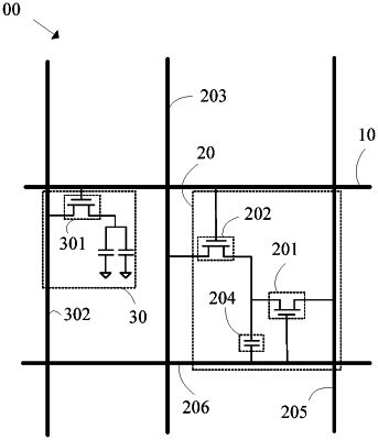
1. A display panel, comprising:
a substrate;
a circuit, disposed on the substrate, and comprising:
a light control device, comprising:
a photosensitive thin film transistor; and
a switching thin film transistor, comprising a drain electrically connected to a source of the photosensitive thin film transistor;
a display device, comprising a display thin film transistor;
a scan line, electrically connected to a gate of the switching thin film transistor and a gate of the display thin film transistor to enable the light control device and the display device to operate simultaneously; and
a photosensitive reading line, electrically connected to a source of the switching thin film transistor;
a conductive portion, disposed over the light control device and connected to the photosensitive reading line;
a conductive connection portion, connecting the conductive portion and the switching thin film transistor;
a plurality of multiplexing electrodes, disposed on the substrate, wherein each of the plurality of multiplexing electrodes is configured as a common electrode during a first time period and configured as a touch electrode during a second time period non-overlapped with the first time period;
a plurality of metal portions, disposed at a side of the plurality of multiplexing electrodes close to the substrate and corresponding to the plurality of multiplexing electrodes in a one-to-one manner; and
a plurality of connection portions, disposed corresponding to the plurality of multiplexing electrodes in a one-to-one manner, wherein two ends of each of the plurality of connection portions are connected to a corresponding multiplexing electrode of the plurality of multiplexing electrodes and a corresponding metal portion of the plurality of metal portions, respectively, to electrically connect the corresponding multiplexing electrode to the corresponding metal portion.
|