| CPC G06F 3/04164 (2019.05) [G06F 3/0412 (2013.01); H05K 1/181 (2013.01); H01R 12/52 (2013.01); H05K 2201/10128 (2013.01); H05K 2201/10378 (2013.01); H05K 2201/10515 (2013.01); H05K 2201/10522 (2013.01); H05K 2201/1053 (2013.01)] | 16 Claims |

|
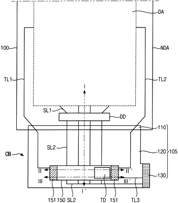
1. A circuit board comprising:
a base substrate separate from and configured to connect to a display panel; and
a connection structure disposed on the base substrate, and connected to the base substrate by an accessing part, the connection structure including:
a first connection electrode disposed in a first layer;
a second connection electrode disposed in the first layer;
a third connection electrode connected to the first connection electrode and disposed on the first connection electrode, and disposed in a second layer;
a fourth connection electrode connected to the second connection electrode and disposed on the second connection electrode, and disposed in the second layer, and
a signal electrode disposed in the first layer,
wherein the signal electrode is connected to a signal line, which transmits a signal from the base substrate to the display panel to display an image on the display panel,
wherein the display panel includes a touch sensing layer disposed thereon,
wherein the touch sensing layer is connected to the first connection electrode by a first touch line, and is connected to the second connection electrode by a second touch line, and
wherein at least one of the first touch line and the second touch line includes a resistance value increasing portion, and the resistance value increasing portion has a meander shape.
|