| CPC G06F 12/1081 (2013.01) [G06F 13/24 (2013.01)] | 10 Claims |

|
1. A storage system processing a request from a host apparatus, comprising:
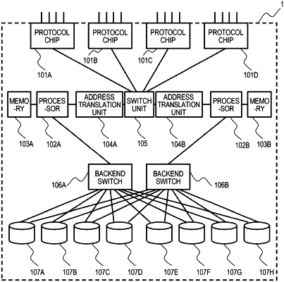
a storage controller, wherein the storage controller comprises:
a protocol chip controlling a protocol for communication with the host apparatus;
a plurality of processors performing control of the storage system;
a first address translation unit translating between a first memory address used by a first processor among the plurality of processors and a second memory address used by the protocol chip; and
a second address translation unit translating between a third memory address used by a second processor among the plurality of processors and the second memory address,
wherein the protocol chip transmits the request from the host apparatus to the first processor through the first address translation unit,
wherein the first processor transmits a response to the request from the host apparatus transmitted from the protocol chip, to the protocol chip through the first address translation unit,
wherein, when the first processor stops processing, an instruction to transmit the request from the host apparatus to the second processor is transmitted to the protocol chip,
wherein, after receiving the instruction to transmit the request from the host apparatus to the second processor, the protocol chip transmits the request from the host apparatus to the second processor through the second address translation unit,
wherein the second processor transmits the response to the request from the host apparatus transmitted to the second processor, to the protocol chip through the second address translation unit,
wherein the second memory address is being used by a third processor,
wherein the protocol chip transmits an interrupt signal to the third processor,
wherein, when receiving the interrupt signal from the protocol chip, the third processor transmits the interrupt signal to the first processor,
wherein, when the first processor stops the processing, the instruction to transmit the interrupt signal to the second processor is transmitted to the third processor, and
wherein, after receiving the instruction to transmit the interrupt signal to the second processor, when receiving the interrupt signal from the protocol chip, the third processor transmits the interrupt signal to the second processor through the second address translation unit.
|