| CPC G06F 11/366 (2013.01) [G06F 11/073 (2013.01); G06F 11/0754 (2013.01); G06F 11/0793 (2013.01)] | 20 Claims |

|
1. An electronic device comprising:
a memory storing instructions; and
a processor connected to the memory and configured to execute the instructions to:
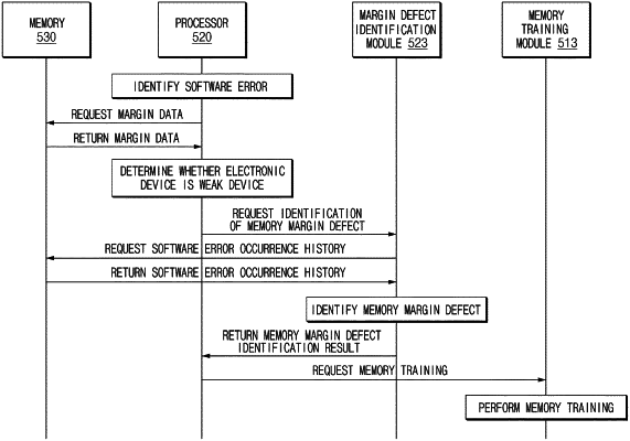
based on a software error occurring in the electronic device, determine whether attribute data set in relation to a memory margin of the electronic device corresponds to a specified value,
based on determining that the attribute data corresponds to the specified value, identify a software error occurrence history stored in the memory,
identify a defect associated with a memory margin configuration set for the memory based on the occurring software error and the software error occurrence history, and
change the memory margin configuration by performing memory training on the memory based on the identification of the defect,
wherein the memory margin comprises information about a driving voltage and information about latency associated with data transmission.
|