US 12,130,657 B2
Semiconductor device
Jae Gon Lee, Seongnam-si (KR); Jae Young Lee, Hwaseong-si (KR); and Se Hun Kim, Yongin-si (KR)
Assigned to Samsung Electronics Co., Ltd., (KR)
Filed by SAMSUNG ELECTRONICS CO., LTD., Suwon-si (KR)
Filed on Sep. 21, 2023, as Appl. No. 18/471,844.
Application 18/471,844 is a continuation of application No. 18/099,077, filed on Jan. 19, 2023, granted, now 11,860,687.
Application 18/099,077 is a continuation of application No. 17/372,122, filed on Jul. 9, 2021, granted, now 11,592,861, issued on Feb. 28, 2023.
Claims priority of application No. 10-2020-0100969 (KR), filed on Aug. 12, 2020; and application No. 10-2021-0072230 (KR), filed on Jun. 3, 2021.
Prior Publication US 2024/0012446 A1, Jan. 11, 2024
Int. Cl. G06F 1/10 (2006.01)
CPC G06F 1/10 (2013.01) 20 Claims
OG exemplary drawing
 
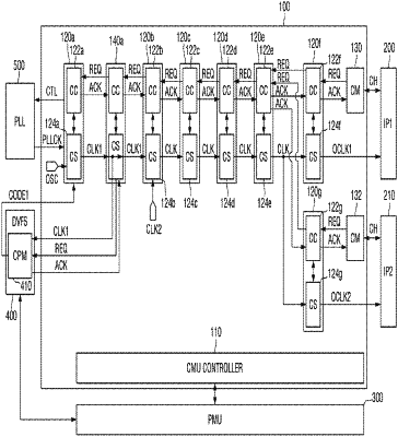
1. A semiconductor device comprising:
a critical path monitor (CPM) configured to monitor a clock signal provided to a processor;
a clock manager circuit configured to perform a clock stopping for the CPM in response to receiving a first request indicating the processor does not want to receive the clock signal and perform a clock activating for the CPM in response to receiving a second request indicating the processor wants to receive the clock signal; and
a dynamic voltage frequency scaling (DVFS) circuit configured to,
control a phase lock loop (PLL) to adjust a frequency of the clock signal provided to the processor using the CPM, and
control an external device to adjust a voltage supplied to the processor.