US 12,130,654 B2
Area-efficient scalable memory read-data multiplexing and latching
Amir Javidi, Hillsboro, OR (US); Daniel Cummings, Austin, TX (US); and Glenn Starnes, Austin, TX (US)
Assigned to Intel Corporation, Santa Clara, CA (US)
Filed by Intel Corporation, Santa Clara, CA (US)
Filed on Dec. 30, 2022, as Appl. No. 18/092,074.
Application 18/092,074 is a continuation of application No. 17/338,550, filed on Jun. 3, 2021, granted, now 11,619,963.
Application 17/338,550 is a continuation of application No. 16/386,070, filed on Apr. 16, 2019, granted, now 11,029,720, issued on Jun. 8, 2021.
Prior Publication US 2023/0137508 A1, May 4, 2023
Int. Cl. G06F 1/06 (2006.01); G06F 1/3206 (2019.01); G11C 7/10 (2006.01)
CPC G06F 1/06 (2013.01) [G06F 1/3206 (2013.01); G11C 7/1039 (2013.01); G11C 7/1075 (2013.01)] 23 Claims
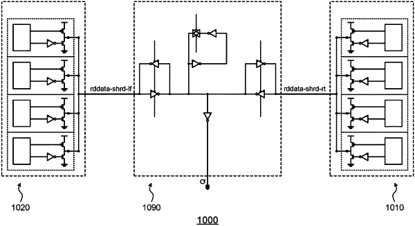
OG exemplary drawing
 
1. An apparatus, comprising:
a first true data signal line and a first complement data signal line of a first side of a memory array;
a second true data signal line and a second complement data signal line of a second side of the memory array;
a true NAND circuit coupled to the first true data signal line and the second true data signal line;
a complement NAND circuit coupled to the first complement data signal line and the second complement data signal line;
latch keeper circuitry coupled to the true NAND circuit; and
an output port coupled to the latch keeper circuitry.