| CPC G03G 15/5037 (2013.01) [G03G 15/5054 (2013.01); G03G 15/75 (2013.01)] | 14 Claims |

|
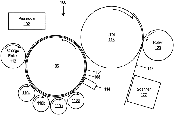
1. A print apparatus comprising:
a photoconductive surface to receive a latent image representative of an image to be printed onto a printable substrate;
a plurality of print components, each print component having a surface movable relative to the photoconductive surface, wherein a current or voltage is to be applied between the print component surface and the photoconductive surface;
a scanner to scan the printable substrate having the image printed thereon; and a processing circuitry to:
measure the current or voltage between each print component surface and the photoconductive surface;
responsive to detecting a deviation in the measured current or voltage from a reference current or voltage in respect of any of the plurality of print components, determine that there exists a defect associated with the photoconductive surface;
determine, based on an amount of the deviation of the measured current or voltage from the reference current or voltage, an indication of a size of the defect; and
determine, from a scan of the printable substrate, a location of the defect on the printable substrate and a corresponding location of the defect with respect to the photoconductive surface.
|