| CPC G02F 1/133308 (2013.01) [G02F 1/13452 (2013.01); G02F 1/13456 (2021.01); G02F 1/136286 (2013.01); G02F 1/1368 (2013.01); G03F 7/0005 (2013.01); G09G 3/3208 (2013.01); G09G 3/36 (2013.01); H01L 27/124 (2013.01); H01L 27/1259 (2013.01); G09G 2310/0264 (2013.01)] | 20 Claims |
|
1. A display apparatus comprising:
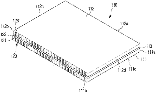
a first substrate having a rectangular shape comprising an upper end, a left end, a right end, and a lower end, and further comprising a plurality of wiring pads extending to the lower end;
a display layer provided on a front surface of the first substrate;
a second substrate provided on a front surface of the display layer, the second substrate comprising an upper end, a left end, and a right end coincident with the upper end, the left end, and the right end of the first substrate, and further comprising a lower end shorter than the lower end of the first substrate, wherein the second substrate is configured relative to the first substrate to expose the plurality of wiring pads of the first substrate;
a plurality of side wiring pads provided on the lower end of the first substrate and the lower end of the second substrate, wherein each respective side wiring pad is connected to a respective a wiring pad of the plurality of wiring pads; and
a display driving circuit connected to the plurality of side wiring pads,
wherein the plurality of side wiring pads are bent to correspond to a step formed by the lower end of the first substrate and the lower end of the second substrate, and
wherein each wiring pad of the plurality of wiring pads is in contact with at least one side wiring pad of the plurality of side wiring pads.
|