| CPC G02B 27/0172 (2013.01) [G02B 5/3016 (2013.01); G02B 27/4205 (2013.01)] | 20 Claims |

|
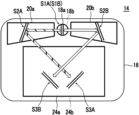
1. A light guide element comprising a light guide plate and a first incidence diffraction element, a second incidence diffraction element, a first emission diffraction element, and a second emission diffraction element that are provided on the light guide plate,
wherein the first incidence diffraction element and the second incidence diffraction element diffract incident light in different directions to be incident into the light guide plate,
the first emission diffraction element emits light that is diffracted by the first incidence diffraction element and propagates in the light guide plate from the light guide plate,
the second emission diffraction element emits light that is diffracted by the second incidence diffraction element and propagates in the light guide plate from the light guide plate,
a period of a diffraction structure of the first incidence diffraction element and a period of a diffraction structure of the second incidence diffraction element are different from each other,
a period of a diffraction structure of the first emission diffraction element and a period of a diffraction structure of the second emission diffraction element are different from each other,
the first emission diffraction element and the second emission diffraction element are disposed at a position where the first emission diffraction element and the second emission diffraction element overlap each other in a plane direction of a main surface of the light guide plate, and
a periodic direction of the diffraction structure of the first emission diffraction element and a periodic direction of the diffraction structure of the second emission diffraction element intersect with each other.
|