| CPC G01R 31/31924 (2013.01) [G01R 31/31905 (2013.01)] | 11 Claims |

|
1. A test interface circuit, comprising:
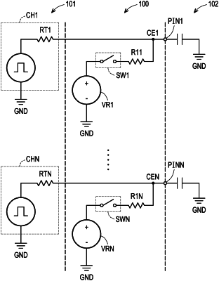
N switches, wherein a first end of each of the N switches is coupled to each of N test connection ends, a second end of each of the N switches receives a reference voltage, and N is a positive integer;
N first resistors, wherein each of the N first resistors is coupled to each of the N switches in series between each of the N test connection ends and the reference voltage,
wherein each of the N switches is controlled by each of N control signals to be turned on or cut off; and
N control signal generators, respectively coupled to the N switches, for providing the N control signals, wherein each of the N control signal generators comprises:
a second resistor, having a first end receiving an operation voltage;
a third resistor, having a first end receiving the operation voltage;
a transistor, having a first end coupled to a second end of the second resistor, having a control end coupled to a second end of the third resistor, and having a second end coupled to a reference ground end, wherein the control end of the transistor receives an input signal; and
a fourth resistor, coupled between the control end and the second end of the transistor.
|