| CPC C30B 29/406 (2013.01) [C23C 16/34 (2013.01); C30B 25/183 (2013.01); C30B 28/12 (2013.01); H01L 21/0242 (2013.01); H01L 21/0243 (2013.01); H01L 21/02433 (2013.01); H01L 21/02458 (2013.01); H01L 21/0254 (2013.01); H01L 21/02609 (2013.01); H01L 21/0262 (2013.01); H01L 33/007 (2013.01); H01L 33/12 (2013.01); H01L 33/32 (2013.01)] | 19 Claims |
|
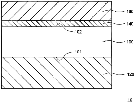
1. A nitride semiconductor template, comprising:
a substrate having a diameter of 2 inches or more and having a front surface and a back surface opposite to the front surface;
a back side semiconductor layer provided on a back surface side of the substrate, comprising a polycrystalline group III nitride semiconductor, and having a linear expansion coefficient different from a linear expansion coefficient of the substrate; and
a front side semiconductor layer provided on a front surface side of the substrate, comprising a monocrystalline group III nitride semiconductor, and having a linear expansion coefficient different from a linear expansion coefficient of the substrate,
wherein surface roughness on the back surface of the substrate is larger than surface roughness on the front surface of the substrate,
a thickness of the front side semiconductor layer is more than 20 μm,
the front side semiconductor layer has no cracks, and
root mean square roughness on a front surface of the front side semiconductor layer is 2 nm or less in as-grown state.
|