| CPC C25D 5/34 (2013.01) [C23C 18/1653 (2013.01); C25D 5/022 (2013.01); C25D 7/00 (2013.01); C25D 7/0614 (2013.01); C25D 7/0678 (2013.01); G11B 5/486 (2013.01); H01J 37/32403 (2013.01); H01J 37/32825 (2013.01); H05K 1/053 (2013.01); H05K 3/182 (2013.01); G11B 5/484 (2013.01); H05K 2203/0709 (2013.01); H05K 2203/095 (2013.01)] | 9 Claims |

|
1. A method of producing a flexible circuit, the method comprising:
directing a gas that is perpendicular to a surface of the flexible circuit, the gas penetrating a first electrode located above the flexible circuit, the flexible circuit being part of a web that includes a plurality of circuits including the flexible circuit, wherein the flexible circuit includes a flexible metal substrate and a dielectric polymer layer disposed on the metal substrate;
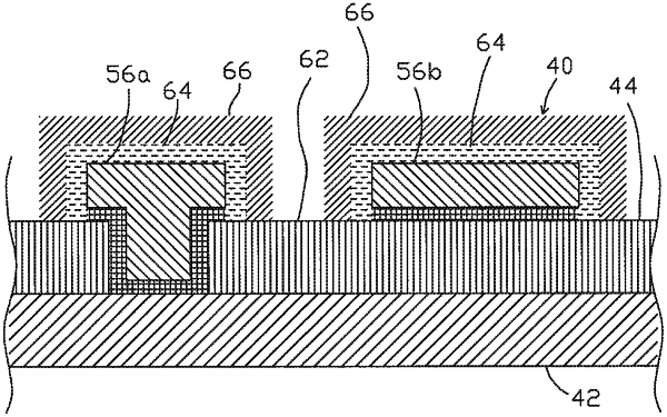
depositing a seed layer on the dielectric polymer layer, wherein an opening is formed on the dielectric polymer layer to expose a portion of the flexible metal substrate;
covering a portion of the seed layer with a patterned photoresist layer;
electroplating a conductive metal onto portions of the seed layer not covered by the patterned photo-resist layer to form a plurality of conductive traces, wherein a first conductive trace of the plurality of conductive traces are formed in the opening of the dielectric polymer layer that establishes an electrical connection between the at least one conductive trace and the flexible metal substrate and a second conductive trace of the plurality of conductive traces is at least partially disposed over the dielectric polymer layer;
plating another conductive metal onto the plurality of conductive traces by electroless plating;
stripping away the patterned photoresist layer to expose the portion of the seed layer; etching away the exposed portion of the seed layer to expose a portion of a surface of the dielectric polymer layer;
forming a dielectric polymer coating over each of the plurality of conductive traces and at least part of the dielectric polymer layer such that a part of the dielectric polymer layer is exposed between conductive traces of the plurality of conductive traces;
applying an alternative voltage to the first electrode to generate a voltage differential between the first electrode and a second electrode connected to a ground, wherein the voltage differential creates an atmospheric plasma from the gas, the second electrode located below the flexible circuit; and
treating the surface of the flexible circuit and the exposed portion of the surface of the dielectric polymer layer with the atmospheric plasma, the second electrode including a roller that is in contact with the web and supports and propels the web including at least the flexible circuit through the atmospheric plasma in a direction that is perpendicular to the gas, wherein the atmospheric plasma removes conductive contaminants from the exposed portion of the surface of the dielectric polymer layer between adjacent conductive traces.
|