| CPC B23B 27/14 (2013.01) [B22F 3/12 (2013.01); B22F 7/008 (2013.01); B22F 7/06 (2013.01); B22F 2005/001 (2013.01); B22F 2302/406 (2013.01); B23B 2226/315 (2013.01)] | 5 Claims |

|
1. A diamond joined body comprising a hard substrate and a polycrystalline diamond layer arranged on the hard substrate, wherein
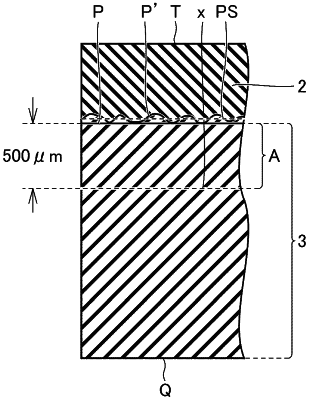
an area ratio of carbon grains in a region of the hard substrate is greater than 0% and less than 0.03%, the region being a region enclosed by an interface between the hard substrate and the polycrystalline diamond layer and an imaginary line x in a cross section parallel to a normal direction of the interface, the imaginary line x being parallel to the interface on the hard substrate side and having a distance of 500 μm from the interface,
wherein the hard substrate does not include rhenium, and
wherein the hard substrate includes tungsten carbide grains having a volume average grain size of not less than 0.1 μm and not more than 3 μm.
|