US 12,127,489 B2
Integrated circuit structure
Tai-Yen Peng, Hsinchu (TW); Hui-Hsien Wei, Taoyuan (TW); Wei-Chih Wen, Hsinchu County (TW); Pin-Ren Dai, Hsinchu County (TW); Chien-Min Lee, Hsinchu County (TW); Han-Ting Tsai, Kaohsiung (TW); Jyu-Horng Shieh, Hsinchu (TW); and Chung-Te Lin, Tainan (TW)
Assigned to TAIWAN SEMICONDUCTOR MANUFACTURING CO., LTD., Hsinchu (TW)
Filed by TAIWAN SEMICONDUCTOR MANUFACTURING CO., LTD., Hsinchu (TW)
Filed on Feb. 17, 2023, as Appl. No. 18/170,947.
Application 18/170,947 is a continuation of application No. 17/369,671, filed on Jul. 7, 2021, granted, now 11,588,107.
Application 17/369,671 is a continuation of application No. 16/983,928, filed on Aug. 3, 2020, granted, now 11,063,217, issued on Jul. 13, 2021.
Application 16/983,928 is a continuation of application No. 16/397,871, filed on Apr. 29, 2019, granted, now 10,734,580, issued on Aug. 4, 2020.
Application 16/397,871 is a continuation of application No. 15/799,416, filed on Oct. 31, 2017, granted, now 10,276,794, issued on Apr. 30, 2019.
Prior Publication US 2023/0210028 A1, Jun. 29, 2023
Int. Cl. H10B 63/00 (2023.01); H10B 61/00 (2023.01); H10N 50/01 (2023.01); H10N 50/80 (2023.01); H10N 70/00 (2023.01); H10N 70/20 (2023.01)
CPC H10N 70/884 (2023.02) [H10B 61/22 (2023.02); H10B 63/30 (2023.02); H10B 63/82 (2023.02); H10B 63/84 (2023.02); H10N 50/01 (2023.02); H10N 50/80 (2023.02); H10N 70/023 (2023.02); H10N 70/063 (2023.02); H10N 70/24 (2023.02); H10N 70/245 (2023.02); H10N 70/826 (2023.02); H10N 70/8416 (2023.02); H10N 70/8833 (2023.02)] 20 Claims
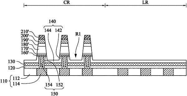
OG exemplary drawing
 
1. An integrated circuit (IC) structure comprising:
a substrate comprising a memory region and a logic region;
a first dielectric structure over the memory region;
a second dielectric structure laterally extending from the first dielectric structure to over the logic region, wherein the second dielectric structure has a thickness less than a thickness of the first dielectric structure;
a first via structure extending through the first dielectric structure, wherein a top segment of the first via structure is higher than a top surface of the first dielectric structure; and
a first memory cell structure over the first via structure.