| CPC H10N 50/80 (2023.02) [H10B 61/00 (2023.02); H10N 50/01 (2023.02)] | 20 Claims |

|
1. A method comprising:
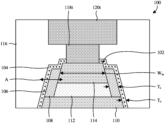
forming a data storage element and a top electrode stacked over a bottom electrode layer with the data storage element between the top electrode and the bottom electrode layer;
forming a sidewall spacer on a first common sidewall formed by the data storage element and the top electrode;
performing a first etch into the bottom electrode layer with the sidewall spacer in place to form a bottom electrode underlying the data storage element;
forming an etch stop layer covering the top electrode and lining a second common sidewall formed by the sidewall spacer and the bottom electrode;
depositing an intermetal dielectric (IMD) layer covering the etch stop layer and having a bottom surface recessed relative to the data storage element;
performing a second etch into the IMD layer to form a via opening overlying the top electrode, wherein the second etch stops on the etch stop layer; and
performing a third etch to extend the via opening to the top electrode;
forming a via extending through the etch stop layer to the top electrode and filling the via opening; and
wherein the forming of the sidewall spacer comprises doping the sidewall spacer, and/or wherein the forming of the etch stop layer comprises doping the etch stop layer, to reduce charge accumulation at an electric dipole between the etch stop layer and the sidewall spacer.
|