| CPC H10K 59/131 (2023.02) [G09G 3/3241 (2013.01); H10K 59/1216 (2023.02); H10K 59/122 (2023.02); H10K 59/65 (2023.02); G09G 2300/0465 (2013.01); G09G 2300/0819 (2013.01); G09G 2300/0842 (2013.01); G09G 2360/14 (2013.01); H01L 27/124 (2013.01); H10K 59/1213 (2023.02); H10K 59/35 (2023.02)] | 16 Claims |

|
1. A display substrate, comprising:
a base substrate; and
a plurality of sub-pixels disposed on the base substrate, wherein each sub-pixel comprises a pixel driving circuit, and the pixel driving circuit comprises a writing transistor, a compensation transistor, a first reset transistor, and a storage capacitor,
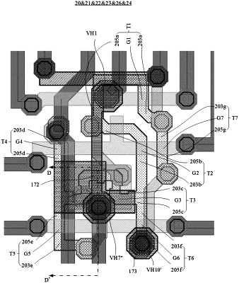
wherein the display substrate comprises a semiconductor layer, a first conductive layer and a second conductive layer disposed in sequence on the base substrate, wherein a gate of the writing transistor, a gate of the compensation transistor, and a gate of the first reset transistor are located in the first conductive layer and are implemented as a continuous integral structure; an active layer of the writing transistor, an active layer of the compensation transistor and an active layer of the first reset transistor are located in the semiconductor layer; a first storage capacitor electrode of the storage capacitor is located in the first conductive layer, and a second storage capacitor electrode of the storage capacitor is located in the second conductive layer.
|