US 12,127,413 B2
Magnetoresistive random access memory and method for fabricating the same
Kun-Ju Li, Tainan (TW); Tai-Cheng Hou, Tainan (TW); Hsin-Jung Liu, Pingtung County (TW); Fu-Yu Tsai, Tainan (TW); Bin-Siang Tsai, Changhua County (TW); Chau-Chung Hou, Tainan (TW); Yu-Lung Shih, Tainan (TW); Ang Chan, Taipei (TW); Chih-Yueh Li, Taipei (TW); and Chun-Tsen Lu, Tainan (TW)
Assigned to UNITED MICROELECTRONICS CORP., Hsin-Chu (TW)
Filed by UNITED MICROELECTRONICS CORP., Hsin-Chu (TW)
Filed on Feb. 23, 2023, as Appl. No. 18/113,070.
Application 17/223,024 is a division of application No. 16/531,108, filed on Aug. 4, 2019, granted, now 11,004,897, issued on May 11, 2021.
Application 18/113,070 is a continuation of application No. 17/223,024, filed on Apr. 6, 2021, granted, now 11,621,296.
Claims priority of application No. 108123743 (TW), filed on Jul. 5, 2019.
Prior Publication US 2023/0200088 A1, Jun. 22, 2023
Int. Cl. H10B 61/00 (2023.01); G11C 11/16 (2006.01); H01F 10/32 (2006.01); H01F 41/34 (2006.01); H10N 50/01 (2023.01); H10N 50/80 (2023.01)
CPC H10B 61/00 (2023.02) [G11C 11/161 (2013.01); H01F 10/3254 (2013.01); H01F 41/34 (2013.01); H10N 50/01 (2023.02); H10N 50/80 (2023.02)] 9 Claims
OG exemplary drawing
 
1. A semiconductor device, comprising:
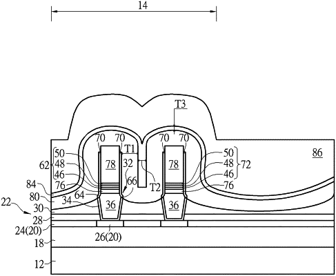
a first magnetic tunneling junction (MTJ) and a second MTJ on a substrate;
a first ultra low-k (ULK) dielectric layer on the first MTJ and the second MTJ, wherein the first ULK dielectric layer comprises a first thickness;
a passivation layer on the first ULK dielectric layer, wherein the passivation layer extending vertically between the first MTJ and the second MTJ comprises a second thickness, the passivation layer on top of the first MTJ comprises a third thickness, and the second thickness is greater than the third thickness; and
a second ULK dielectric layer on the passivation layer.