US 12,127,411 B2
Cocktail layer over gate dielectric layer of FET FeRAM
Rainer Yen-Chieh Huang, Changhua County (TW); Hai-Ching Chen, Hsinchu (TW); and Chung-Te Lin, Tainan (TW)
Assigned to Taiwan Semiconductor Manufacturing Company, Ltd., Hsinchu (TW)
Filed by Taiwan Semiconductor Manufacturing Company, Ltd., Hsinchu (TW)
Filed on Aug. 2, 2023, as Appl. No. 18/363,986.
Application 17/873,236 is a division of application No. 17/168,342, filed on Feb. 5, 2021, granted, now 11,581,334, issued on Feb. 14, 2023.
Application 18/363,986 is a continuation of application No. 17/873,236, filed on Jul. 26, 2022, granted, now 11,818,896.
Prior Publication US 2023/0380177 A1, Nov. 23, 2023
Int. Cl. H01L 29/40 (2006.01); H01L 21/28 (2006.01); H01L 23/522 (2006.01); H01L 29/51 (2006.01); H01L 29/66 (2006.01); H01L 29/78 (2006.01); H10B 51/30 (2023.01)
CPC H10B 51/30 (2023.02) [H01L 23/5226 (2013.01); H01L 29/40111 (2019.08); H01L 29/516 (2013.01); H01L 29/6684 (2013.01); H01L 29/78391 (2014.09)] 20 Claims
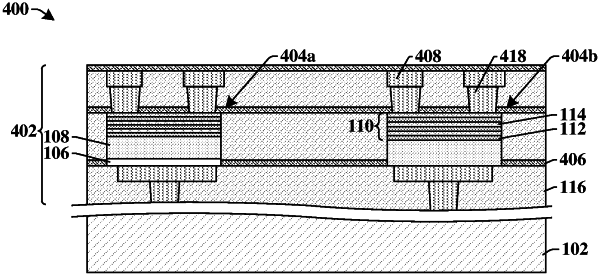
OG exemplary drawing
 
1. A semiconductor device, comprising:
a gate electrode over a substrate;
a semiconductor structure over the substrate and comprising a plurality of cocktail layers and a plurality of active layers that are stacked and vertically alternate with the cocktail layers, wherein the cocktail layers individually comprise a mixture of a first material and a second material, wherein the active layers individually comprise a third material, and wherein the first, second, and third materials each comprise a different metal element;
a gate dielectric layer between the semiconductor structure and the gate electrode; and
a source contact and a drain contact on the semiconductor structure.