| CPC H10B 10/125 (2023.02) [H01L 29/0665 (2013.01); H01L 29/42392 (2013.01); H01L 29/78696 (2013.01); H10B 10/18 (2023.02)] | 20 Claims |

|
1. A semiconductor structure, comprising:
a substrate; and
first and second SRAM cells over the substrate,
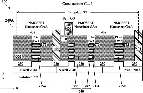
wherein the first SRAM cell includes a first inverter having a first pull-up GAA transistor coupled to a first pull-down GAA transistor and a second inverter having a second pull-up GAA transistor coupled to a second pull-down GAA transistor, the first and the second inverters are cross-coupled to form a first data storage nodes, the first SRAM cell further includes first and second pass-gate GAA transistors for accessing the first data storage nodes, each of the first and the second pass-gate GAA transistors has a first channel width, each of the first and the second pull-down GAA transistors has a second channel width, and a ratio of the second channel width to the first channel width is in a range of 1.05 to 1.5,
wherein the second SRAM cell includes a third inverter having a third pull-up GAA transistor coupled to a third pull-down GAA transistor and a fourth inverter having a fourth pull-up GAA transistor coupled to a fourth pull-down GAA transistor, the third and the fourth inverters are cross-coupled to form a second data storage nodes, the second SRAM cell further includes third and fourth pass-gate GAA transistors for accessing the second data storage nodes, each of the third and the fourth pass-gate GAA transistors has a third channel width, each of the third and the fourth pull-down GAA transistors has a fourth channel width, and the third and the fourth channel widths are substantially same, and
wherein the fourth channel width is larger than the second channel width, and
wherein each of the first and the second pull-up GAA transistors has a fifth channel width, each of the third and the fourth pull-up GAA transistors has a sixth channel width, and a ratio of the sixth channel width to the fifth channel width is in a range of 1.05 to 1.5.
|