| CPC H05K 1/141 (2013.01) [H05K 3/36 (2013.01); H05K 2201/09754 (2013.01); H05K 2201/10325 (2013.01); H05K 2201/10977 (2013.01)] | 12 Claims |

|
1. A printed circuit board connecting device (1) for connecting a first and a second printed circuit board (3, 5), the printed circuit board connecting device (1) comprising:
a non-conductive plate (21) having a top side and a bottom side; and
a plurality of interface connections (23) which are arranged in the plate (21) so as to be spaced apart from one another,
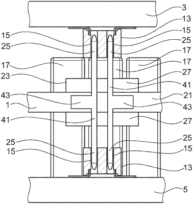
wherein each interface connection (23) has grouped-together conductors (41) which extend through the non-conductive plate (21) and which are laterally enclosed by the non-conductive plate material and the end regions of which protruding on the top side and bottom side from the non-conductive plate (21) can be fixed to interfaces (13) of the first and second printed circuit boards (3, 5) to be connected, and therefore the conductors (41) form both a mechanical and an electrical connection between the interfaces (13) of the first and second printed circuit boards (3, 5),
wherein the interface connections (23) are each defined by a base (27) that protrudes on the top side of the non-conductive plate (21) and/or a base (27) that protrudes on the bottom side of the non-conductive plate (21),
wherein the base (27) is a thickened portion of the non-conductive plate (21) on its top side and/or bottom side,
wherein the end regions are configured as at least first and second bar-shaped plug pins (25) that are configured to be fixed in sockets (15) of the interfaces (13),
wherein the grouped-together conductors (41) have a widened portion (43) that is encapsulated by the non-conductive plate (21), and wherein the grouped together conductors (41) are connected to the non-conductive plate (21) in a form-fitted and/or materially bonded manner,
wherein the printed circuit board connecting device (1) is configured to be disposed between the first printed circuit board (3) and the second printed circuit board (5) in such a manner that the top side of the non-conductive plate (21) is configured to face a bottom side of the first printed circuit board (3) and the bottom side of the non-conductive plate (21) is configured to face a top side of the second printed circuit board (5), and wherein the printed circuit board connecting device (1) is configured to extend in a parallel manner with respect to the first and second printed circuit boards (3, 5), and
wherein the first bar-shaped plug pin (25) has a first surface having the widened portion (43) and the second bar-shaped plug pin (25) has a first surface having a second widened portion (43) facing away from the widened portion (43) of the first surface of the first bar-shaped plug pin (25), wherein the first bar-shaped plug pin (25) has a second surface facing opposite the first surface of the first bar-shaped plug pin (25) and the second bar-shaped plug pin (25) has a second surface facing the second surface of the first bar-shaped plug pin (25), and wherein the second surfaces of the first and second bar-shaped plug pins (25) are free of a widened portion such that the second surfaces of the first and second bar-shaped plug pins (25) are parallel to one another.
|