|
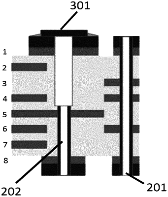
1. A multilayer printed circuit board intended to connect electronic components, the multilayer printed circuit board comprising a stack of a plurality of conductive layers, the conductive layers comprising two surface layers and one or more internal layers, separation between two neighbouring conductive layers being ensured by means of an electrically insulating layer, the printed circuit board comprising one or more counterbored holes, each counterbored hole being configured to electrically connect one of the two surface layers to one or more internal layers and comprising a portion with metallization opening onto one of the two surface layers and a portion without metallization opening onto the other surface layer, the portion with metallization and the portion without metallization of a counterbored hole extending in a direction perpendicular to a layer stacking plane, wherein the multilayer printed circuit board further comprises one or more metal pads, each metal pad being joined to one of the two surface layers so as to occult the portion without metallization of a corresponding counterbored hole.
|
