| CPC H04N 25/76 (2023.01) [H04N 25/47 (2023.01); H01L 27/14612 (2013.01)] | 20 Claims |

|
1. A solid-state imaging element, comprising:
a plurality of first photoelectric conversion elements arranged side by side in a first region;
a plurality of second photoelectric conversion elements arranged side by side in a second region adjacent to the first region;
a plurality of current-voltage conversion circuits that each converts currents output from the plurality of first photoelectric conversion elements or the plurality of second photoelectric conversion elements into voltages; and
a plurality of address event detection circuits that each detects a change in the voltages output from the plurality of current-voltage conversion circuits,
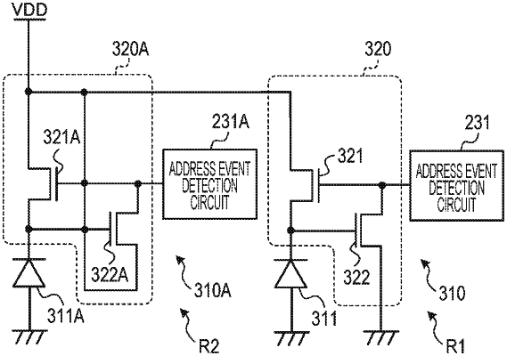
wherein at least either the current-voltage conversion circuits or the address event detection circuits connected to the second photoelectric conversion elements prevent output of signals based on the currents output from the second photoelectric conversion elements,
wherein internal potentials of at least either the current-voltage conversion circuits or the address event detection circuits connected to the second photoelectric conversion elements are fixed,
wherein the current-voltage conversion circuits connected to the second photoelectric conversion elements include a plurality of transistors, and
wherein the internal potentials of the current-voltage conversion circuits connected to the second photoelectric conversion elements are fixed by short-circuiting the plurality of transistors.
|