| CPC H04N 25/709 (2023.01) [H01L 27/14612 (2013.01); H01L 27/14643 (2013.01); H04N 25/707 (2023.01)] | 10 Claims |

|
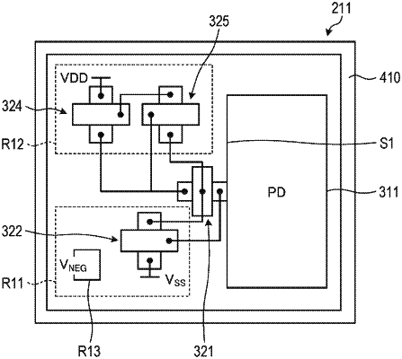
1. A solid-state imaging device, comprising:
a plurality of photoelectric conversion elements arranged side by side in a first region;
a plurality of current-voltage conversion circuits that convert currents output from the plurality of photoelectric conversion elements into voltages, respectively;
a plurality of address event detection circuits that detect changes in the voltages output from the plurality of current-voltage conversion circuits, respectively;
first ground wiring that is provided in a second region located outside the first region and that supplies first ground potential to the plurality of photoelectric conversion elements; and
second ground wiring that is provided in the second region and that supplies second ground potential having a voltage value different from a voltage value of the first ground potential to the plurality of current-voltage conversion circuits,
wherein each current-voltage conversion circuit in the plurality of current-voltage conversion circuits includes a loop-shaped source follower circuit,
the source follower circuit including:
a first transistor, wherein a source of the first transistor is directly connected to a photoelectric conversion element of the plurality of photoelectric conversion elements, and wherein the source of the first transistor is connected to a substantial center of the photoelectric conversion element in a cross section obtained by cutting a stacked substrate in a stacking direction of the stacked substrate on which the plurality of photoelectric conversion elements is formed; and
a second transistor, wherein a gate of the second transistor is directly connected to the photoelectric conversion element, and wherein a drain of the second transistor is connected to a gate of the first transistor.
|