| CPC H04B 1/04 (2013.01) [H01L 23/66 (2013.01); H03F 3/24 (2013.01); H01L 2223/6644 (2013.01); H03F 1/565 (2013.01); H03F 2200/165 (2013.01); H03F 2200/451 (2013.01)] | 14 Claims |

|
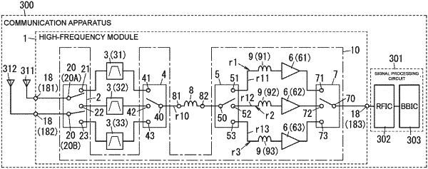
1. A high-frequency module comprising:
a plurality of filters configured to be selectively connected to an antenna terminal;
a plurality of amplifiers;
a first switch having a first common terminal and a plurality of first selection terminals, the plurality of filters being respectively connected to the plurality of first selection terminals;
a second switch having a second common terminal and a plurality of second selection terminals, the plurality of amplifiers being respectively connected to the plurality of second selection terminals;
a plurality of signal paths, each signal path being between one of the plurality of filters and a corresponding one of the plurality of amplifiers, and each of the plurality of signal paths sharing a common path portion between the first common terminal of the first switch and the second common terminal of the second switch,
a first inductor connected to the common path portion;
a plurality of second inductors, each of the plurality of second inductors being in a different signal path and in a portion of the respective signal path other than the common path portion; and
a mounting substrate having a first main surface and a second main surface that are opposite to each other,
wherein the first inductor is a surface mount inductor located on the first main surface of the mounting substrate, and
wherein the plurality of second inductors are each:
an inductor disposed within an integrated circuit (IC) chip comprising the plurality of amplifiers, or
an inductor comprising a conductive pattern in or on the mounting substrate.
|